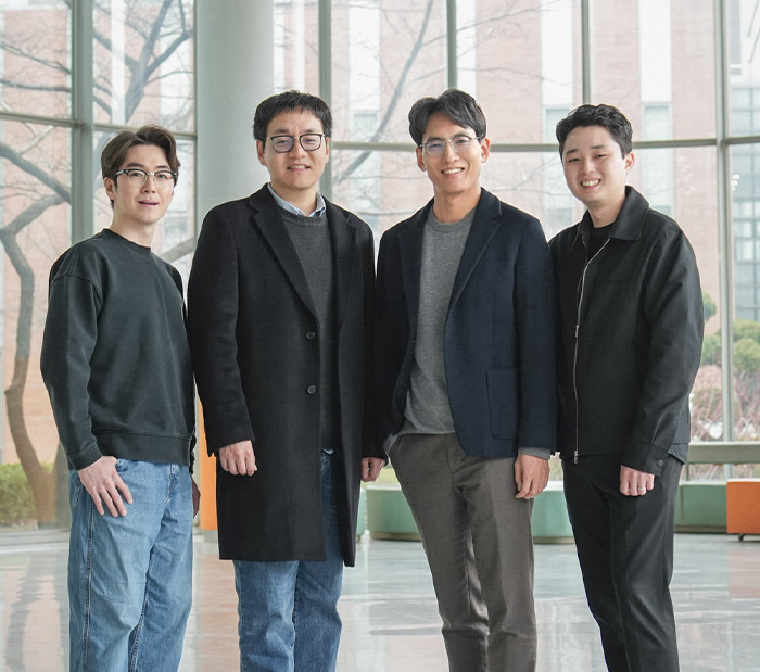
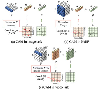
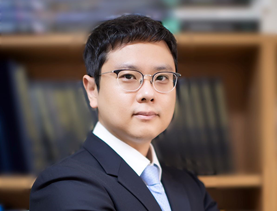
Development of two novel methodologies for efficient representation of complex 3D scenes
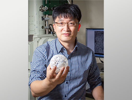
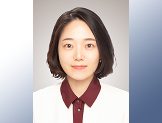
전자전기/인공지능학과 Prof. 박은병, 고종환
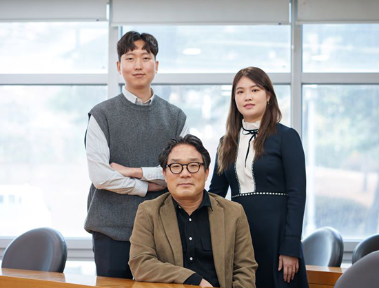
Prof. Eunbyung Park and Prof. Jong Hwan Ko
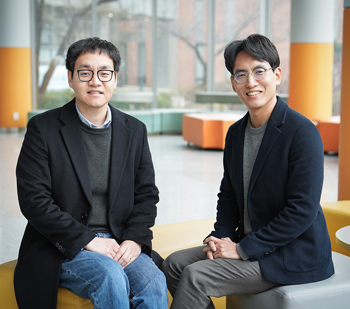
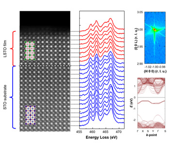
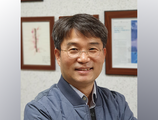
Predicting and demonstrating of hidden metastable phase in transition metal oxide
Advanced Materials Science and Engineering Prof. LEE, JAICHAN
Bongwook Chung
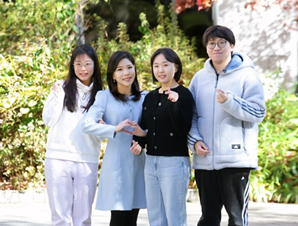
Undergraduate student majoring in English Language and Literature and Library and Information Science, published an SSCI paper (supervised by Professor Na-yeon Kim) ▲ (from left) Ziying Li, a doctoral student, Professor Na-yeon Kim, Chaejin Lee (English Language and Literature), Seong-hyun Byun (Library and Information Science) The research paper led by Professor Na-yeon Kim of the Department of English Language and Literature, titled "Zero-derivation in Korean: the effect of covert structure in real-time processing," has been published in the December issue of the SSCI journal 'Frontiers in Psychology: Psychology Of Language.' The paper explores the linguistic and cognitive aspects of words with ambiguous grammatical categories, revealing their subtle syntactic structures through both linguistic and cognitive psychological methodologies. Notably, this paper holds significant meaning as it is a collaborative effort, not only involving Ziying Li, a doctoral student, but also featuring contributions from undergraduate students, Chae-jin Lee, a third-year English Language and Literature major, and Seong-hyun Byun, a fourth-year student majoring in Library and Information Science. The research focuses on the phenomenon of 'zero-derivation' in Korean. For instance, in Korean, the word '밝다' ('bright') can be used both as an adjective and a verb. While previous studies have explored the phenomenon of adjectives and verbs sharing grammatical categories, there has been no experimental study determining whether such categories are distinct or if the verb '밝다' derives from the adjective '밝다.' This study analyzes the process by which the verb '밝다' is derived from the adjective '밝다' through cognitive psychological methodologies. It reveals that we can easily understand sentences by being sensitive to the unseen syntactic structures and the derivation process of grammatical categories. The study suggests that sentences with omitted words, i.e., those not visible or audible, also possess delicate and intricate syntactic structures. Humans can recognize these structures, enabling them to quickly comprehend sentences involving omissions. The research team is currently collaborating with professors from foreign language departments at the University of Toronto, Northwestern University, and the National University of Singapore to systematize various syntactic experiments that elucidate the interaction mechanism between these subtle syntactic structures and cognitive processes. Additionally, ongoing research at our university's Artificial Intelligence Convergence Institute, led by Professor Kwang-soo Kim, explores whether artificial intelligence can acquire these unique language characteristics exhibited by humans. Professor Na-yeon Kim expressed, "It's commendable that two undergraduate research students and a doctoral student have passionately contributed to this research for over a year, dedicating weekends. In the future, I plan to further expand opportunities for collaborative research with students in the field of interdisciplinary research between English language and cognitive psychology through the Language and Cognition Lab." ※ Author: Kim, N., Li, Z., Byeon, S., & Lee, C. ※ Title: Zero-derivation in Korean: The Effect of Covert Structure in Real-time Processing. ※ Journal: Frontiers in Psychology,14, 1230927
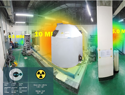
Professor Jong-seo Chai (Department of Electrical and Electronic Engineering) has been selected for the Ministry of Science and ICT's leading research center (CRC) new project in 2023 -focus on developing broadband precision radiation measurement and utilizing metaverse for visualization -creating detailed radiation maps in emergency situations Professor Jong-seo Chai from the Department of Electrical and Electronic Engineering has been selected for the Ministry of Science and ICT's leading research center (CRC) new project in 2023. The project, titled "Metaverse-Based Radiation Safety ICT Research Center," will conduct groundbreaking research on fully visualizing radiation for the first time in the world. The goal is to implement radiation data measured in a specific space into virtual reality or mixed reality and visualize it using metaverse technologies such as AR and VR. This aims to provide a realistic radiation map. Creating accurate and reliable models of radiation levels has been a challenging task in academia, requiring vast amounts of data collection and complex calculations. To pursue research on radiation visualization based on metaverse, the research team will explore innovative approaches to visual representation based on engineering technologies for safety. The team aims to establish a new approach to radiation safety by securing independent technology that combines efficiency and stability in radiation work and utilizing radiation visualization technology. This is expected to contribute to the safe utilization of radiation in our society, including public health, radiation safety, and safety education. Professor Jong-seo Chai, who oversees the research, stated, "By creating detailed radiation maps, even in national emergencies such as radiation terrorism, we will be able to effectively prepare and plan for such situations."
Prof. Yong Taik Lim’s Research Team (SAINT) Developed the World’s First K-nanoadjuvant Prof. Yong Taik Lim’s research team (SAINT) developed the world’s first kinetically activating nanoadjuvant (K-nanoadjuvant), which enables therapeutic immune cells to generate effective antitumor immunity without exhaustion. The research results were published in Nature Nanotechnology (IF: 39.213), a world-renowned academic journal in the field of multidisciplinary science. Various drugs capable of effective innate immune induction, such as toll-like receptor (TLR) agonists, have been developed throughout the history of oncology. Although these drugs contribute to immune activation, they also cause immunotoxicity and exhaustion of immune cells, resulting in ineffective cancer immunotherapy overall. To address these issues, Prof. Lim's team designed a nanoliposome-based novel TLR7/8a (timely activating TLR7/8 agonist; t-TLR7/8a) for the first time and revealed the efficacy of K-nanoadjuvant fabricated in combination with various TLR agonists. A nanoliposome-based K-nanoadjuvant is a novel immune function-modulating platform that not only maximizes immune cell activation but also overcomes immune cell exhaustion induced by excessive immune responses. Such effect was achieved by coordinating optimized time, order, and combinatorial code of two different immunostimulants with different mechanisms of action which induce different signal transduction routes. K-nanoadjuvant solves the problem of current immunostimulants and has a high potential for clinical application, as previous research has proven the safety of nanoliposome-based platforms in the human body. Researchers expect K-nanoadjuvant to be applied to immune checkpoint inhibitors unresponsive patient group, the latest anticancer therapeutic drug, and can be used as a next-generation anticancer therapeutic drug that can prevent recurrence/metastasis. ※ Paper Title: A nanoadjuvant that dynamically coordinates innate immune stimuli activation enhances cancer immunotherapy and reduces immune cell exhaustion ※ Journal: Nature Nanotechnology
Unveiling the Hidden Secrets to Crystal Facets – Perovskite Solar Cell Stability against Moistures Improved Dramatically - Discovered the most stable facet (111) against moistures, posted exclusively on US weekly scientific journal, Science - Prof. Nam Gyu Park’s research team, the first to discover Perovskite Crystal Facet (exposed side of crystal) stable against humidity - Maintaining more than 95% of initial efficiency in 2000 hours of moisture exposure experiment ▲ (from the left) Prof. Nam-Gyu Park, Prof. Seok Jun Kwon, Prof. Michael Grätzel, Dr. ChunQing Ma Prof. Nam-Gyu Park, (SKKU Department of Chemical Engineering Chair and Institute of Sungkyun Energy Science Technology Director, corresponding author) and Dr. ChunQing Ma (first author), cooperated with Prof. Seok Jun Kwon (SKKU Department of Chemical Engineering, co-corresponding author), and Prof. Michael Grätzel (Switzerland École Polytechnique Fédérale de Lausanne) to announce their research result about their success in the discovery of stability against moisture depending on Perovskite* Crystal Facets**, producing the film with the most humidity-stable facet (111) and, finally the developing the solar cell that maintained 95% of its original capacity during 2000 hours of humidity exposure experiment on journal Science, January 13th (local time). * Perovskite: Crystal with chemical formula ABX3. In the crystal, A and X have 12-fold coordination while B and X have 6-fold coordination. ** Crystal Facet: The geometrically flat side of a crystal that has a patterned structure of atom arrangement. Perovskite solar cells are solar cell technologies that include organic-inorganic hybrid perovskite light-absorbing materials. In 2012, Prof. Park’s research team first developed a solid Perovskite Solar Cell with 9.7% efficiency, pioneering a new academic field called ‘Perovskite Photovoltaics’. Due to this Perovskite Solar Cell development research credits, Clarivate nominated him for the 2017 Novel Prize candidate. The perovskite light absorption layer for solar cells can be manufactured at a relatively low temperature of 150°C or less using a simple solution process. When a generally known solution process is used, perovskite crystals have polycrystalline properties in the formed film, and crystal facets are not well developed. Prof. Park’s research team succeeded in producing perovskite films with well-developed (100) and (111) crystal facets using additive methods, revealing the photoelectric current dependence according to the facets. In this study, for the first time, they found that moisture stability depends on the facet when the perovskite film is exposed to moisture. In particular, (100) facets are very vulnerable to moisture, but (111) facets are found to be stable to moisture. Theoretical calculations have shown that (111) facets have better water stability than (100) facets because the adhesion (or wetting energy) of water is relatively low on (111) facets. Also, spectroscopy and X-ray diffraction were used to find that a strong bond with water occurs in the moisture-sensitive (100) facet, resulting in a perovskite phase transition from alpha to delta phase, resulting in loss of light absorption characteristics. Based on the investigation of the cause of the difference in moisture stability according to facets, it is necessary to develop a film composed of (111) facets to enhance the water stability of the Perovskite Solar Cell. Thus, Prof. Park used an additive called ‘Cyclohexylamine’ to create a Perovskite film of more than 98% (111) facet composition. Testing the stability against moistures under a relative humidity of 30%~40% environment for about 2000 hours (1938 hours), the results showed that solar cells with (111) facet dominant Perovskite film maintained 95% of initial efficiency. The results of this study were supported by the Ministry of Education, Science and Technology and the Korea Research Foundation (NRF-2021R1A3B1076723) and are expected to significantly improve the life of perovskite solar cells and contribute to commercialization. ※ Paper Title : Unveiling facet-dependent degradation and facet engineering for stable perovskite solar cells ※ Journal: Science
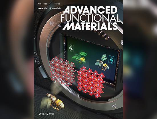
Prof. Il Jeon’s Research Team (SAINT) Develops High-Speed Lead-free Perovskite Photodetector - Developed Tin-based perovskite to identify noise suppression principles - Selected as the cover paper for Advanced Functional Materials ▲ Prof. Il Jeon (SAINT) / Dr. Gyu Seon Kim The domestic research team has developed lead-free perovskite material-based photodetector which can detect light much faster than conventional ones. * Perovskite: A crystal structure of a mineral found in the Ural Mountains, Russia, in 1839. Perovskite structure has high electric charge transportation and light absorption characteristics, gathering attention for its potential to be the future material for solar cells. * Photodetector: The light-detecting device in the image sensor, light sensor, etc. Prof. Il Jeon and Dr. Gyu Seon Kim’s research team (SAINT) joint with Prof. Dong Hwan Wang and Dr. Woong Sik Jang (Chung-Ang University), announced their success in implementing the passivation process on photodetector for improving the stability of perovskite thin film by suppressing noise efficiently. * Passivation: The process of passivating a film by forming a film through treatment such as using a solvent to prevent the reaction at the surface *Noise: undesired distortion of input signals such as external interference. Electric signal that impedes accurate detection. Recently, perovskite materials that can control absorbance according to their composition are in the spotlight as future-generation photosensitive materials that can replace inorganic photosensitive materials but were facing difficulties in commercialization due to the harmful effects of lead. Conventional lead-based perovskites have a relatively low binding force between lead ions and halogen ions, allowing ions to move easily in the structure, which has caused noise generation and also has been the major cause of deterioration in photodetector performance by facilitating injection of external charges. Accordingly, the joint research team succeeded in developing high-quality non-lead perovskite materials by applying passivation technology that can stably form thin films by utilizing tin materials, an ingredient that can replace lead. Unlike conventional lead-based materials, tin-based perovskite materials have shown superiority in suppressing noise generation within photodetector by limiting the movement of internal ions through the strong binding energy of tin and halogen ions. Tin based non-lead Perovskite Photodetector Structure and Noise Suppression effect due to Tin content As a result, it was possible to verify the implementation of a non-lead perovskite photodetector with the excellent photosensitive ability and fast speed by blocking the external current flow that degrades the performance. This study is expected to enable the simultaneous implementation of eco-friendly technology and performance improvement technology due to the next-generation photodetector with tin-based perovskite material. It is expected to contribute to the development of related technologies as it is expected to be applicable in the field of future photoelectric conversion devices and displays based on various perovskite materials. The research results of Prof. Jeon’s research team are published in the material field’s global academic journal, Advanced Functional Materials, on December 16th and were selected to be the cover thesis for its research excellence.
Prof. Hwan Su Yoon’s Research Team (Department of Biological Sciences) Discovers Red Algae Evolution Strategy in Extreme Environment Adaptation - Confirmed various extreme environment adaptation procedures of Cyanidiophyceae Prof. Hwan Su Yoon (Department of Biological Sciences, corresponding author) and Dr. Chung Hyun Cho (first author), have announced the discovery of the genome evolution procedure of photosynthesis eukaryotic adaptation to extreme environment. * Eukaryon: Has a nucleus surrounded by a nuclear membrane and consists of other various cell organelles inside the cell membrane. Undergoes mitosis. All the other microorganisms other than germs and viruses belong to this group. ** Genome: The complete set of genes or genetic material information required for biological phenomena in a cell or organism. Cyanidiophyceae is the first classification to split from red algae species, ramifying from their common ancestor to adapt to extreme environments such as volcano or thermal spring. Volcano or thermal spring has high temperatures (45~60 ℃), acid concentrations (pH 0~4), and rich heavy metals, forming a harsh environment for organisms to develop in general. However, Cyanidiophyceae is the only eukaryotic organism found in this extreme environment and is the key to the evolution process of organisms that develop in harsh conditions. Living things in extreme environments are constantly exposed to various external physical and chemical stresses, which interfere with biomaterial metabolism. The research team newly decoded the genome of three kinds of Cyanidiophyceae at the chromosome level to find out how Cyanidiophyceae adapted to this environment. Genetic evolution and adaptability in heavy metal environments were analyzed through genetic comparative analysis which yielded an interesting fact that bacteria and archaea genes of various origins were found in the genome of Cyanidiophyceae. Cyanidiophyceae externally obtained a gene that neutralizes heavy metals such as arsenic and mercury from bacteria through horizontal gene transfer and later confirmed that they adapted to extreme environments by increasing the number of genes internally through subtelomeric gene duplication. * Subtelomeric Gene Duplication: Concept of genetics that refers to the transfer of genotypes from individual to individual without reproduction. Can transfer beyond the species. All key genes related to microRNA, one of the representative gene expression control mechanisms of eukaryotes in Cyanidiophyceae, have disappeared, and in addition, some of the mechanisms unnecessary for extreme environmental survival have been lost in the classification. Moreover, through the evolution process, it was confirmed that the proteins of Cyanidiophyceae were modified and adapted suitably for a high-temperature acidic environment. The genetic evolution strategy employed to adapt to the polar environment is used in all Cyanidiophyceae species, but the detailed gene and genome composition also differed among Cyanidiophyceae species. Through this study, the team suggested that the differences in genes and genomes that occurred during the speciation process affected the differences in the habitat environment of each species within their current extreme environment. Prof. Yoon said, “Cyanidiophyceae have strong vitality to adapt to extreme environments and can be used in various applications such as biological heavy metal decontamination, system/synthesis biology, genetic engineering, etc.” This research was supported by Korea Research Foundation's Mid-size Research Support and Plant Biological Rhythm Leading Research Center. The research results were published in the global academic journal Nature Communications (IF=17.694) on January 4th (Wed). ▲ Cyanidiophyceae-living Sulfur Thermal Spring water of high temperature (45~60 ℃), acidity (pH 0~4), and heavy metal content ▲ Extreme Environment Adaptation System of Cyanidiophyceae
Prof. Suk Ho Bhang (Department of Chemical Engineering) Developed Conductive Hydrogel Customized for Tumor Detection and Removal -Reactive oxygen species responsive hydrogel-based tumor excision technology -Wireless monitoring constructed through conductivity-based machinery and electronic control Prof. Suk Ho Bhang’s research team (Department of Chemical Engineering, first author: Gwang-Bum Im) developed reactive oxygen species responsive conductive hydrogel sensors that can be controlled mechanically and electronically as a result of joint research with Prof. Sung Young Park’s research team (Korea National University of Transportation). Tumor, or cancer, is a serious threat to human health because of its incidence and fatality rate. Early diagnosis and prevention are the global objective since detecting and excluding all kinds of malignant tissue through surgical operation possess difficulties. The conventional cancer detection technology which has its basis in tumor markers such as immunosensor or immunoassay is measured in clinical laboratories which use sophisticated techniques and thus is not suitable for clinical purposes, not to mention its excessive time in between body fluid acquirement and analysis result. Therefore, the need for a new method that can acquire detailed information fast without professional or special knowledge has been on the rise, and this research focused on a portable detection method that can selectively and accurately detect cancer environments. Hydrogel is a typical biocompatible material that has been used for biosensing due to its characteristic of adjustable pores for fluid absorption. Nanoparticle mixed conductive hydrogel especially can detect electronic signals related to various stimuli such as temperature, oxidation-reduction, pH, light, pressure, and strain. However, research focused on clinical diagnostic tests based on hydrogel that reacts to extracellular pH and reduced glutathione (GSH) is very rare in history, and research of cancer microenvironment based on pressure-strain detecting hydrogel is unprecedented. Prof. Bhang’s research team developed a tumor microenvironment selective conductive hydrogel sensor based on reactive oxygen species (ROS)-responsive carbon dot (CD)-embedded hydrogel. This sensor provides tumor selectivity by dismantling diselenide crosslinks within the ROS-rich tumor microenvironment. The existence of cancer cells can be distinguished by monitoring abnormal pressure and strain signals. Also, dsCD-Hydrogel can be used with wireless devices, allowing it to monitor hydrogel’s sensor information at the tumor-containing section and collect data using smartphones. (Figure 1) ▲ [Figure 1] Hydrogel-based sensing system that can be monitored through Prof. Bhang's smartphone The ROS scavenging activity of the dsCD-Hydrogel decreased tumor volume. Furthermore, NIR irradiation via PTT abolished the tumor, which was verified by the downregulation of tumor hypoxia by vascular endothelial growth factor (VEGF) and hypoxia-inducible factor 1α (HIF-1α) expression. (Figure 2) ▲ [Figure 2] Data on the elimination of active oxygen and photothermal effects in mice Prof. Bhang and Prof. Park, explained, “We will establish a hydrogel sensor system suitable for cancer treatment and furthermore confirm actual applicability for quick detection of tumors.” The research result was published online on December 5th in the globally renowned chemical engineering field academic journal, Chemical Engineering Journal (IF: 13.273). ※ Paper Title: ROS-responsive mechanically and electronically controllable conductive hydrogel sensor with NIR modulated photothermal therapy ※ Journal: Chemical Engineering Journal ※ Paper Link: https://doi.org/10.1016/j.cej.2022.140729
Prof. Jeong Min Baik’s Research Team (Dept. of Advanced Materials Science and Engineering) Suggests Fundamental Solution to Thermoelectric Energy Harvesting - Achieved World’s best Output Voltage with Frictional charge and Thermoelectric Carrier Coupling effect - Published in Energy field International Journal, Advanced Energy Materials Prof. Jeong Min Baik’s Research Team (Dept. of Advanced Materials Science and Engineering) joined with Prof. Jae Sung Son’s (Dept. of Materials Science and Engineering, UNIST) research team, developed a technology that semi-permanently improves the performance of thermoelectric energy harvester through frictional charge and thermoelectric carrier coupling effect. Thermoelectric energy harvesting technology is a technology that produces energy with potential difference created by the temperature difference of a material’s bisection during external heating and is assessed to be a suitable solution to converting waste heat produced in the industrial field to sustainable energy production, having a simple structure, low maintenance cost, and high reliability as its strength. Until now, the energy conversion efficiency was minute due to contact resistance between the heat source and thermoelectric elements and the internal resistance of the elements. Moreover, optimization of the output could not be achieved because of the limits set by the material’s power factor and thus output level for commercialization was not accomplished. * Power factor: Performance index used when assessing electricity power density produced by the thermoelectric module, calculated by multiplying the square of the materials’ Seebeck coefficient by the electrical conductivity * Seebeck coefficient: Coefficients that correlate the voltage differences generated inside the material per unit temperature. Materials with a high Seebeck coefficient are known to be thermally conductive. To break through the limit mentioned above, Prof. Baik’s research team developed and attached polyimide-based material which can contain high negative charge semi-permanently at lower temperature part of BiSbTe-based thermoelectric element which has the highest ZT value (thermal conduction performance index) at room temperature and induced fusion effect with carriers inside the thermoelectric elements. Through this, they yielded 4 times the output increment compared to the existing models and achieved the world’s best output voltage (2 times the existing one). The benefit of this research is that this technology does not require external physical friction effects to create a negative charge so it can work semi-permanently. Prof. Baik said, “This study presents a new direction to improve the low output voltage and energy conversion efficiency, which are the limitations of conventional thermoelectric energy harvesting, and shows excellent performance not only for energy harvesting but also for thermoelectric cooling.” This research's result was published in December, in the energy field international academic journal ‘Advanced Energy Materials (IF: 29.698). Prof. Baik’s research team has applied for two patents related to this research and is continuing to research how to apply thermoelectric energy harvesting in various fields. This research was supported by Mid-sized Research Projects and BRIDGE R&D Projects of the Korea Research Foundation. ※ Paper Title: Boosted Output Voltage of BiSbTe-Based Thermoelectric Generators via Coupled Effect between Thermoelectric Carriers and Triboelectric Charges ※ DOI: 10.1002/aenm.202202987
Prof. Seung Uk Son’s Research Team (Department of Chemistry) Developed Frictional Electricity Harvesting Core-Shell Structure Synergy Material ▲ (from the left) Prof. Seung Uk Son, Dr. Changwan Kang, Jina Park (Master’s degree student) The 'Nanoporous Molecular Network' is known to be ‘multifunctional’ for its high heat stability and contact surface area, making it suitable for applications in an absorbent, sensor, catalyst, battery, and drug delivery. Chemistry Prof. Seung Uk Son’s research team has developed that frictional electricity harvesting core-shell structured materials are synthesized by applying a microporous polymer network to the shell of the material with a coupling reaction of ZnO nanorod aggregate core material. The resulting core-shell structure has a core of 440 nm diameter, composed of ZnO nanoparticles, and a microporous polymer network shell with 45 nm thickness. The ZnO nanorod in the core has 10~15nm thickness and 50~70 nm length. Frictional electricity occurs when two materials with different electron conditions experience friction, allowing electron transfer on the surface. Recently, various research on materials or devices are being conducted to harvest this frictional electricity to utilize it as a new source of energy. Prof. Son’s research team applied ZnO, known to have polar arrangement due to piezoelectric effect, on a frictional electricity harvesting device to investigate how internal piezoelectric material affects the device during contact. In this study, the researchers observed frictional electricity harvesting capacity of the core cell material was significantly increased through comparative studies between piezoelectric materials and frictional electricity harvesting materials. In addition, the friction electricity harvesting ability was much higher when compared to the case where the piezoelectric material and the friction electricity harvesting material were simply mixed. It is believed that the polarity generated in the core cell material at the contact moment helps to transmit electrons for generating friction electricity. In other words, it can be interpreted that the polar environment due to electron transfer helps the phenomenon along with the synergy efficiency of the core cell structure. Prof. Son also synthesized various functional materials based on nano-porous polymer networks and applied those to various fields such as battery materials, carbon-neutral eco-friendly metal catalysts, photocatalysts, sensors, and drug delivery materials. Related studies were published in the top 10% journals and were selected as cover papers. The first author, Dr. Changwan Kang, received support from the Department of Chemistry BK21 Four project group, SKKU Post-Doc training program, and is currently continuing his research at McGill University as Post-Doc researcher. The co-author, Master’s degree student Jina Park, is supported by the Department of Chemistry BK21 Four project group. This research was conducted in cooperation with Prof. Sang Woo Kim, and Advanced Materials student Dong Min Lee. Prof. Son’s research results have been supported by the Mid-Sized Research Support Project of the Korea Research Foundation and were published in the highest rank journal in the Chemistry field, Angewandte Chemie Int. Ed. (IF=16.823), in 2022. ※ Paper Title: Core-Shell ZnO@Microporous Organic Polymer Nanospheres as Enhanced Piezo-Triboelectric Energy Harvesting Materials
Prof. Whasun Lim Discovers Endometriosis Suppression Efficacy of Melatonin Prof. Whasun Lim’s research team (Department of Biological Sciences) disclosed a result showing that melatonin can cause mitochondrial dysfunction in endometriosis lesions and disease cell lines and specifically inhibit cell proliferation by regulating tiRNA expression. This research, in which Prof. Lim participated as a corresponding author, was conducted in cooperation with Prof. Gwonhwa Song’s research team (Korea University), Prof. Sunwoo Park’s research team (Gyeongsang National University), and Prof. Hee Seung Kim’s research team (Seoul National University). The research result was published online in the international expert journal in endocrinology, brain sciences, physiology field, Journal of Pineal Research (IF: 12.081, JCR field Top 3.09%), on November 18th. Endometriosis is a disease that occurs in about 15% of childbearing-age women, in which endometrium tissues grow abnormally on the ovary, oviduct, and peritoneum, ensuing not only atypical genital bleeding but also infertility. Surgeries and hormone therapies are being conducted to cure the disease, but recurrent rates are high and long-term injections are impossible. Melatonin not only controls biological rhythm but is also known to have various physiological activities such as antioxidation and anti-inflammatory. Thus, the research team certified an endometriosis mouse model and confirmed a decrease in the lesion size of the disease according to the treatment of melatonin. Moreover, using endometriosis epithelial cell lines and substrate cells separated and cultivated from the patient tissue, it was confirmed that melatonin inhibits proliferation, induces apoptosis, and decreases ATP synthesis through mitochondrial membrane potential and oxidative phosphorylation changes. Recently, transport RNA fragments (tRF/tiRNAs), a type of small non-coding RNA in living organisms, have been found to have various biological functions such as RNA interference. The research team demonstrated that tiRNAGluCTC and tiRNAAspGTC were associated with the proliferation of endometriosis in the lesion of mouse endometriosis originating from a patient and it was confirmed to suppress the expression of those two tiRNAs according to the treatment of melatonin. The result of this study identified a new efficacy and mechanism to suppress the development of melatonin endometriosis lesions and showed the possibility of new usage as therapeutic material for endometriosis patients. This research was supported by the Ministry of Science and ICT, the National Research Foundation of Korea's Mid-sized Research and Young Researcher Support Project, and the Ministry of Health and Welfare's Korea Health Industry Promotion Agency's Public Medical Technology Research Project. ※ Paper Title: Melatonin inhibits endometriosis development by disrupting mitochondrial function and regulating tiRNAs ※ Journal: Journal of Pineal Research ※ DOI: https://doi.org/10.1111/jpi.12842 ▲ Mechanisms of melatonin inhibiting the development of endometriosis lesions